After my foray into the CBM Plus4 (the worlds most fragile 8-bit computer) I have acquired another A500+ motherboard with battery damage. This feels like coming home and, after the confidence bashing of the Plus4, I've picked myself up and I'm ready to DO THIS! C'MON! RARGH! YEAH!!
Ahem.
 |
| Oooh - a parcel! What's inside? |
 |
| It's only an A500+ motherboard with Agnus and ROM! |
This time the actual board looks relatively unscathed. The same, however, cannot be said for Gary's socket. The pins are green and, er, mostly gone. Just touching the spring contacts resulted in them disintegrating... But amazingly, the solder mask has not been damaged at all which leads me to suspect that the Amiga was stored standing on end and leaning with its keyboard facing towards the floor.
 |
| I spy with my little eye...a borked Gary socket |
 |
| But no solder mask damage. Hmmmm... |
Anyway, this is another 'on the cheap' repair i.e. I have to do this with no additional parts other than what I have available from my previous escapades. Bear this in mind as you read on.
First things first, get Gary's socket off. Now, I don't have a lot of luck removing large chips from boards and I don't know why. It just seems that I haven't got the knack of removing solder completely from the pin holes. I've had some more luck with expensive solder wick but that is, well, expensive. So, I'd decided to bite the bullet and cut Gary's socket off as cleanly as possible with the intention of gluing it back together.
"But what about those disintegrated pins?", I hear you cry. Well, I have somehow ended up with a surplus of 16 pin DIP sockets which have the same style of pins. They are small pieces of spring metal that are pressed into the holes in the plastic socket. It's simple to remove them from the 16 pin sockets and re-insert them into Gary's socket. It is very tedious and I had promised myself I would not do this ever again. But needs must. See
here.
 |
| Pins, lots of them... |
After carefully gluing Gary's socket back together and then re-inserting the pins I soldered it back to the board. Didn't he do well?
 |
| As bright as a shiny new pin(s). |
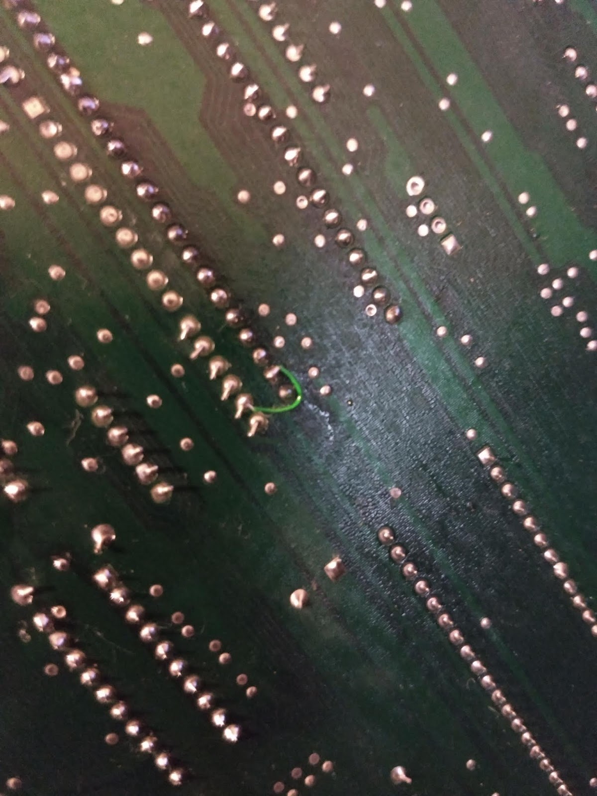
With Gary's socket back on the board I checked to see if there were any broken traces. Another chunk of time taken up with continuity checking, but worth it as I identified one missing connection which was simply fixed with a small wire.
 |
| Broken Gary trace - strange, but fixed. |
Time to dig out the rest of the chips. The board is a straight swap with one of the guys on the Amiga FB group so we did it 'chips out' so to speak. After fishing them all out of the box, and checking I had the right ones - Denis and Agnus are ECS and I have some OCS chips in my spares box - I was ready to rumble. So, the first attempt to boot. Does it boot?
No. Green screen.
Here's a description of the Amiga boot colours, taken from the
classic Amiga wiki.
When the Amiga boots, if it encounters a hardware fault the system will display a solid single coloured screen, or a series of these screens if more than one error is detected.
The following colours are valid for all versions of AmigaDOS since Kickstart 1.3. However, there were several more colours in 1.3 compared to anything included after Kickstart 2.0 was released. However all of the colours listed below are the same for all versions of Amiga kickstart.
- Red - An error in the Kickstart rom as detected.
- Green - An error in the Chip Ram was detected.
- Blue - An error in the custom chip set was detected.
- Yellow - The CPU encountered an error before the system's error-trapping code (the code the calls up the Guru) was in place.
- Black - No CPU detected.
- Grey - CPU Passed the test.
- White - CPU failure.
In addition to colour screen error codes, Guru Meditation error screens are also a common error screen encountered when an Amiga encounters a problem
This is helpful but doesn't give much detail. All I can glean with a green screen is that my chip RAM may be borked. But Agnus may be faulty, or it could be a damaged trace or it could be something else. There is more information available on the actual sequence of startup:
Taken from Lemon Amiga at
this link. I've reproduced it here as this type of info has a habit of disappearing over time...
Amiga Boot Sequence
1. Clear all of the chips of old data.
2. Disable DMA and interrupts during the test.
3. Clear the screen.
4. Check the Hardware to make sure the 68000 is working.
5. Change the screen to Black, screen stays Black (or with red Stripes) if CPU fault.
6. Do a checksum test on all the ROMS.
7. Change screen to Red if ROMs are faulty, or change to Dark Gray if ROMs are OK.
8. Begin the system startup.
9. Check the Ram at $C0000, and move SYS_BASE there.
10. Test all of the chip RAM.
11. Change screen colour to Green if RAM is faulty, or change to Light Grey if RAM is OK.
12. Check to see if the ROM software is coming in OK and being executed.
13. Change colour to White if the software test is OK, stays Light Grey if faulty, or Blueif Custom Chip error.
14. Set up the chip ram to receive data.
15. Link the ROM libraries so the machine can identify connected devices and peripherals.
16. Check for additional memory in these devices and link it to the computer. 16b. Chance screen colour to Yellow if there is an error with external cards/devices.
17. Turn the DMA and Interrupts back on.
18. Start a default task.
19. Check to see if there are additional CPUs on the system, accelerators or a maths coprocessor.
20. Check to see if there CPUs are OK.
21a. If there is an Exception (processor error), or issue reported, the system will reboot.
21b. The Kickstart Image is Displayed showing that the rom has been installed to memory, is running, and everything so far has reported OK.
After this, the ROM GURU trap handler will display errors as codes on the screen.
My A500+ board fails at step 11 i.e. the chip RAM check failed. No great advance there. After poking around at the logic chips (U10, U11, U12 and U13) it was obvious that something was not right with U12. The voltages at the output pins were all very low i.e. non-existent so I decided to start here. This is good as the chips at U12 are cheap - and I already have a couple of spares - and can easily be socketed.
Removing U12 was not easy. The problem is that the leaky battery liquid death reacts with the solder, resulting in a crystalline lump that does not want to melt. After failing miserably to get more than a few pins released I resorted to an articulated pin disconnection tool (a pair of wire cutters). Cutting through the pins on one side allowed the chip to be bent up and, after a few wiggles, the chip came off. It was then a simple matter of flooding the pin area with new solder and using a solder sucker to remove the mixed old crappy stuff and new stuff, pin remains included. Repeat for U10. Once done a simple clean with some IPA was carried out.
Before soldering a socket in, I decided to check continuity again at U12 since this was the chip that took the brunt of the Varta death. The results were not good:
Pin 1 to pin 19 - broken
Pin 2 to U13 pin 2 - broken
Pin 3 to U13 pin18 - broken
Pin 7 to U13 pin 14 - broken
Pin 8 to U13 pin 9 - broken
Pin 11 to U13 pin 12 - broken
Pin 18 to U13 pin 3 - broken
It looks like the battery had eaten a good chunk of the tracks where they are not protected by the solder mask, just at the point where they meet the solder pads (holes) for the pins. Cleaning up with flux, solder and then IPA was probably enough the break the last vestiges of track at these points. I have had this before - see
here.
 |
| Pin 1 looks unhappy |
 |
| Generally unhappy here too. |
 |
| Urgh.. |
 |
| Flippin 'eck. |
OK. At least I now have something to aim at. I'll need link wires on the underside of the board to rectify these broken traces. I also need to break out my box of sockets so I can put in new chips but have the ability to remove them easily.
Next problem. No 20 pin sockets. I do, as I mentioned earlier, have a big bag of 16 pin sockets though. And a pair of wire cutters. And a tube of superglue. Hmmm. I have a cunning plan. What could possibly go wrong? ;)
The sockets are quite brittle so I had to resort to cutting the socket a little bigger and then filing down the rest to avoid cracks. A dab of superglue was perfect to attach these extensions to an unsullied 16 pin socket. The results, while not perfect, are more than acceptable.
 |
| Socket to 'em! (See what I did there?) |
One final point, which I have mentioned before elsewhere in my blogs. When soldering sockets on to the board, always do opposite corner pins first. That way, you can press the socket down onto the board and ensure it's flat before soldering the rest of the pins, otherwise there is a risk it won't be flat and will look like it's making a bid for freedom.
Talking of which, have a look at this chip here - U15. Would you believe that this was from the factory?? It looks like the chip was supposed to have its legs folded under the board, like all the others, but for some reason they only managed to do this on a few of the legs at one end. This allowed the chip to dangle and start to fall out of the board. I'm not sure of the process they used to solder components to these boards but, more by luck than judgement, this chip managed to get soldered and stay soldered..
 |
| U15 - Have you got somewhere else to be? |
Anyway, sockets now sorted.
Now, link wires. I thought I had a stock of kynar type wire which was green and is nice and fine. I had about two inches left. Fortunately, I also have a winding of copper wire which is coated with laquer. This will do nicely instead. All I need to do is scrape off the laquer at each end and solder as normal.
Here's the list:
 |
| Shopping list of new link wires... |
 |
| New link wires installed. Nice. |
So now, with new sockets, links and the addition of a couple of new 74LS244N chips, lets start this Amiga up again. Does it work?
 |
| It's Alive! |
Of course. :)