Sunday, July 24, 2022

Fix it 'til it's broke - The Third

After dealing with a broken Agnus 8375, it was time to turn my attention back to the A500+ board that was still not working.

A500+ Board from HELL

Initially, I had some very odd symptoms. The board would almost appear to boot (with a floppy drive connected). It would run through the sequence of black screen, grey screen, white screen but then no initial Kickstart screen. With a floppy drive connected the drive would show activity as if it was loading data but the screen would stay white. So something weird was going on..

First thing, I tried swapping the main custom chips, just in case one had gone faulty or was starting to fail. This made no difference. In fact, all of the custom chips worked perfectly in the Rev 6 A500 board I have (except Agnus - Rev 6 and Rev 8 Agnii are NOT pin compatible). But then I realised that the A500+ board was no longer getting to the white screen. Now, it would start at black, then dark grey then it would stop. Hmmm.

Given that this is an A500+, the board has had some previous repair, including sockets for U12 and U13. I tried swapping those chips with known working spares. No difference. In fact, things got even worse. Now the board was stuck on a black screen. Doh.

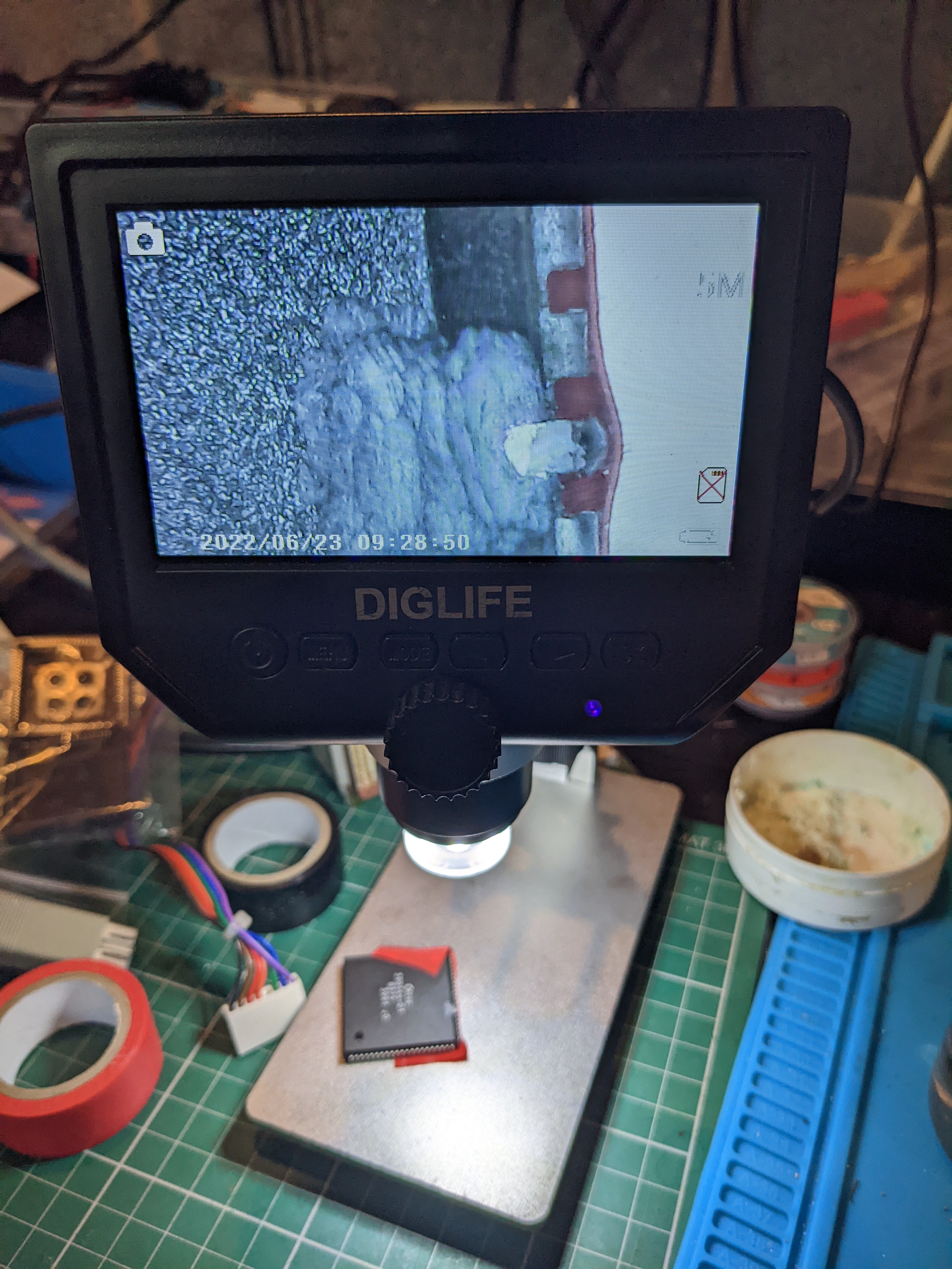
This was beginning to get a bit annoying. I had DiagROM, so hooked up the serial output to see what was happening. The initial test the DiagROM performs is very limited due to only a tiny amount of RAM being available for actual use, but it was showing errors right from the start. 


Well, that doesn't look good.

Then, in a potential case of the Baader-Meinhof phenomenon, Adrian from Adrians's Digital Basement uploaded a video where he had an A500 board (Rev 6) with a potential RAM error and he was using DiagROM to try and solve the issue. As it turned out, his video showed that he did have some dodgy RAM chips but, in my experience, Amiga RAM is pretty hardy and in all the A500+ boards I had previously repaired, I have NEVER had a RAM fault. 

In any case, I went ahead and de-soldered the RAM from my board for two reasons. Firstly, it meant I could put it in a socket, and second, it meant I could test the chips in a handy RAM expansion board that uses four of the same RAM chips with the Rev 6 board along with the excellent Amiga Test Kit from Kier Fraser. Several people on Twitter were convinced that my issues was almost certainly a similar issue to Adrian's i.e. dodgy RAM chips. 

Removing the RAM proved to be a right pain in the behind. Although the battery damage to the RAM was very limited, the solder on many of the legs had reacted with the battery chemicals meaning the solder was dull and would not flow. I managed to damage several traces due to my growing frustration and impatience. Fortunately, the repairs were fairly straightforward and more an annoyance than a major problem.


Spot the damaged traces...doh.

Repairs following my impatience.

Once the sockets were installed and the testing was complete, I was able to see that all of the RAM chips were completely fine. The issues were NOT caused by the RAM. Gah.


Sockets galore

Handy test unit. :)

By this point, several days had gone by and the board was taking up a lot of time. I was convinced that there must be a dodgy trace somewhere so I had generated a multi-tab spreadsheet (everyone loves a spreadsheet) with pin to pin connection details, listing each pin of the major chips and what they were connected to. The 84 pins of Agnus were 'Not Fun'(R). But this also showed no issues with the traces other than previous minor repairs.

One of the comments I had on Twitter came from the most excellent Jan Beta who noted that old and crusty sockets were a major source of problems on previous Amiga boards he had worked on. I took notice of this and decided to solder several chips directly to the board. The chips that received this treatment were:

  • U12
  • U13
  • Gary
  • CPU
  • Even CIA
  • U36 
  • U37 
  • U15 
  • U42
Some of these would normally be soldered to the board anyway but had had sockets fitted as part of previous repairs.

Sadly, this made virtually no difference. What I did notice was that the intermittent RAM fault had disappeared. Interesting... But DiagROM would still get through the memory test and then crash.

Argh! Crashu!

Back to the broken trace theory.

No broken traces.

At some point during all the pulling, pushing, removing, installing two things happened. One, I managed to put it a RAM chip upside down. I have to tell you now that they get bloody hot when that happens. It took me several minutes to realise where the HOT smell was coming from. But the RAM chip in question survived - told you the Amiga RAM was pretty hardy.

RAM the correct way round now..

Two, it broke my 2.04 ROM. By this point I had reached the stage where the 2.04 ROM would show a black screen but the 1.3 ROM would show an immediate green screen. The reason for the black screen on the 2.04 ROM was because it was dead. Completely. Dangnabit.

But the green screen was another clue that this was down to RAM not working properly. Perhaps the Agnus chip wasn't sitting right in the socket. After a careful removal I could see that several of the spring pins in the 'economy' socket I had were bent right into the socket. Perhaps this was the issue. So I fitted another brand new socket.

Damaged socket pins?


Third time's a charm.. no wait..
Third time's a pain in the 

Annnd after all that. No difference. Green screen on the 1.3 ROM and an inevitable crash of DiagROM.

I had had enough at this point. I think I had spent the best part of 20 or 30 hours trying to make the damn thing work. Even DiagROM had stopped working properly and would only display a line of garbage at startup now.

One last ditch effort. I removed the gaggle of chips in the 'data path' i.e. U10, U11, U12 and U13 and fitted brand new sockets. Sadly, I had no 20 pin sockets, but I did have plenty of 24 pin sockets. So, given that this board is staying with me, I decided to just remove the four pins from the end of the socket and solder them on to the board. Providing the chips are inserted fully to the right there is no issue. Of course, if I accidentally put a chip in to the left I will almost certainly kill it but at least they are fairly standard logic chips, if a bit harder to come by these days due to the apocalyptic state of the world...

Shiny sockets

Following this I tried booting it up to see if I could get DiagROM back to where it was with the serial output. 

I nearly fell off my chair. The machine booted flawlessly into DiagROM. 

What. The. Heck.

I was so stunned I forgot to take a picture of DiagROM working. But it worked. I put the ROM back to a normal kickstart, attached a floppy drive with an ATK disk and tried it again.

Standby for action!

Memory! All alone in the moonlight...

So it works. Here's my theory on what was wrong. I think the original problem was that the sockets on the board had corroded/oxidised over the time it's been sat in the box. When I took the sockets off and soldered chips directly to the board (specifically around U10 - U13) I suspect I bridged one or more pins or tracks without realising. Once I took them back off the board and put the sockets on this was cured. And the brand new sockets cured the original issue.

My gut told me it wasn't a RAM fault. I should've listened harder to Jan Beta. :)


Monday, June 27, 2022

Fix it 'til it's broke - Part Deux

I decided that I was going to look at my collection of three floppy drives that have been sat in a box for a long while. They generally work but as no-one uses floppy drives any more I thought I'd explore the art of 'calibrating' a floppy drive, safe in the knowledge that it wouldn't matter too much if I borked one of them doing so. But this is not the subject of this post (next time).

So, break out the spare A500+ motherboard and get that floppy drive plugged in. Annndd... green screen. To be fair, Agnus' socket was busted so that was the first job to sort out. I didn't have any more PLCC sockets so had to order some for a few quid from everyone's favourite, eBay. I won't go into too much detail about the socket replacement other than to say the old one had gone brittle anyway and broke off quite easily.

It's broke.

With a new socket installed I put Agnus back in and tried again. No change so I decided to try and improve the contact of the pins on the chip by gently manipulating the bottom of the legs to push them out slightly. This would, in theory, increase the pressure of the pins into the socket. But, tragedy struck. As I gently pushed pin 81 I noticed it moved far too easily. And then, it fell off.

Oh. 

Arghhhh!!

Pin 81 is HSYNC_ and, as the name suggests, is somewhat important for making sure that Agnus can provide the relevant data at the right time to give a coherent display. 

So, this is it. Agnus is toast. And these particular Agni are the 8375 version, used in the A500+. They are getting more difficult to get at sensible prices (a couple of years ago I bought a complete, non-working A500+ motherboard with chips for a tenner - now just the 8375 Agnus will set you back over £100, if you can find one). 

After posting my woes on twitter, several people suggested using a Dremel (other rotary tools are available) to remove the outer casing above the broken pin and see if a replacement leg could be soldered to whatever was left of the original pin. Given that the chip was broken, I had nothing to lose. A helpful YouTube video from _C64 Customs_ also gave some useful info on what to do - although it isn't specifically about this type of chip. So, I threw caution to the wind. If it didn't work I'd still just have a broken Agnus.

Break out the generic rotary tool from the defunct UK high street electronics supplier. I used the narrowest, pointy milling tool in the box and carefully pinned down Agnus with some insulating tape. 

Grinding away the casing took only a few minutes but I really took my time, allowing the tool to touch the chip very gently and then checking how much material had been removed. Eventually I had managed to expose the part of the original leg in the casing. I carefully cleaned it with IPA and a cotton bud. It was the most terrifying thing I've ever done to a vintage computer chip.

Prior to attempting to solder anything to the exposed leg, I tinned it with a little solder. I still had the original part of the leg that had fallen off so I decided to try and re-use it. It was a bit tricky to get it to stay in place so I used a piece of insulating tape to hold it. This worked pretty well and allowed a good solid blob of solder to flow between the leg and the chip resulting in what looked like to be a good solid repair.

Hole drilled, leg held in place...

Close up of the horror.


Repair complete. Phew!

Close up - a clean is required

Will it work?

There was a big hole in the chip now, even though the leg was repaired. I did not want to leave it like this so I took some epoxy and filled in the hole. It ended up a slightly bigger 'blob' than I had hoped but I was careful to make sure that the epoxy did not interfere with the socket. These sockets are tight.

Agnus pimple

Don't squeeze it! It'll spread!

Epoxy cured - ready for testing

Incidentally, it's worth noting that Fat Agnus (the original version was just 'Agnus') was the absolute largest chip that CBM/MOS could manufacture in the late 1980s. It took the original DIP Agnus and combined various additional bits and pieces - it's all about that cost reduction - including, in further updates, the ability to address chip memory up to 1Mb i.e. memory that can be directly accessed by the custom chips. Hence, Fat Agnus. The 8375 model here is the last ECS version and it can address 2Mb of memory and so is unofficially known as 'Fatter Agnus' or 'Obese Agnus'. 

Now I have a slightly lumpy looking Agnus but I'm actually quite pleased with it. The repair seems pretty sturdy and, other than the pimple, looks almost new. So, to test. Well, first, I put it into the faulty motherboard and the behaviour of that board didn't change. This was a good sign as I would have expected either an unstable image or a green screen if I'd damaged other parts of Agnus. But I have been having trouble fixing that board - another future post - so I threw caution to the wind (again) and carefully removed it from the faulty board and put it into my 'daily driver' A500+ which has the most excellent A500++ re-made board, in purple. 

Agnus' final resting place.

And...

The most excellent FrogFind by Action Retro


AGNUS IS ALIVE! Yes! And it will stay in there as I really don't want to tempt fate by trying to remove it again from a really, really tight socket.

Phew!

Saturday, May 14, 2022

Pin. Pin. Pin. Pin.

Pinouts. Lots of pinouts. Or at least I thought I should properly document the pinouts of the UD-80. This will be the last post on this for a little while as I still have lots of other stuff to look at, including a TV with a faulty SCART input...

First up, SCART.

RGB Cable - 6-pin DIN to SCART

The socket is a 6 pin DIN (240 degrees) socket arranged in the following order:


UD80   Pin            Pin  SCART

GND    1: ---------- : 18  GND

CSYNC  2: ---------- : 20  SYNC (via 470R resistor & 10uf cap)

RED    3: ---------- : 15  RED

GREEN  4: ---------- : 11  GREEN

BLUE   5: ---------- : 7   BLUE

+5V    6: ---------- : 16  RGB BLANKING


Diagram below:

What a lovely diagram.

One key thing here is that I'm not convinced I've got the RGB in the right order. But I would point out that the PX-8 and UD-80 are monochrome, so what difference does it make? :) At least I'm fairly sure that GREEN is in the right place at least...

The CSYNC signal was measuring 5v which is TTL level and a bit over the top for the SCART standard. Sticking the resistor in there, when it's connected to the 75 ohm impedance TV connector, means the output is a much more standard 520mV (thanks to the video by Voultar where he describes the issues with old equipment - see here for that video). The capacitor de-couples any DC bias in the signal.

Here's one I made earlier:

GAAAH!!

And here's one where I put the SCART plug screw on before I re-soldered the plug back on:


Remembered this time...

And, of course, I must not forget the patented DIN plug 'Maximum Assistance Super Hold' (MASH) device i.e. a potatoe:

Hmmmm. Potatoes....

One of the best things to hold the DIN plug so the pins stay in place and don't fall out while you're trying to solder the plug. An excellent tip there. As you can see I did the 8 pin and the 6 pin DIN plugs for the UD-80 with this particular MASH.

Does it work? Of course.

WordStar. You youngsters don't know you're
born. 

A whole 2k free on the A: drive!

Rather interestingly, there is some slight distortion towards the bottom of the screen that looked similar to the composite interference. I suspect this may be related to the UD-80 rather than any issue with my cable but I might investigate at some point.

Next up, the UD-80 connection itself.


UD-80 Serial Cable - 8-pin DIN to 8-pin Mini-DIN


The socket on the front of the UD-80 is an 8-pin 270 degree DIN socket. It can accommodate a 5-pin 180 degree plug since only pins 1 to 5 are actually used. The pins are arranged as follows:

    UD80  Pin            Pin  PX-8 RS232

  GROUND  2: ---------- : 1   GROUND

 DATA IN  1: ---------- : 2   DATA OUT

DATA OUT  3: ---------- : 3   DATA IN

     CTS  5: ---------- : 4   DTR

     DTR  4: ---------- : 5   CTS

     N/C  6:            : 6   N/C

     N/C  7:            : 7   N/C

     N/C  8:            : 8   N/C


The PX-8 can, apparently, use either the RS232 or Serial ports with the UD-80. Everything I have done so far has been with the RS232 port.


UD-80 Operation


The UD-80 replicates and extends the display of the PX-8 from an 8 line LCD display to an 80 or 40 column display with 24 lines via a composite or RGB output (see above for info on RGB). The UD-80 comes with a built-in extension for WordStar to allow the use of the additional screen real-estate. Other applications need to be specifically modified to make use of the additional screen space so they are likely to be few and far between.

This brief 'start-up' guide is based on an PX-8 with no batteries installed and, as such, a lot of the steps taken here would, in the day, only have been required once, particularly if the RAMDisk was fitted (I have one but it's broken. :( ).

Step 1 - Plug in the UD-80 to PX-8 interface cable.
Step 2 - Plug in either composite or RGB monitor according to taste.
Step 3 - Switch on the PX-8 which should default to the start menu.
Step 4 - Switch on the UD-80 which should display a UD-80 banner at the top of the monitor screen.


Step 5 - Run CONFIG.COM and configure 3 blocks of User BIOS space (run the program, select 'B' then press '3' and enter, then ESC twice to get back to the menu).


Step 6 - From the menu or from the CP/M prompt run FILINK.COM
Step 7 - Press 'R' to receive files and then 'Enter' when prompted for a filename.
Step 8 - Press the button on the front of the UD-80. A 'Transmitting...' message should appear and FILINK should indicate it is receiving UD80-DRV.COM and the WSX.COM.


Step 9 - When the downloads in FILINK have completed quit back to the menu and run the UD80-DRV.COM file that will be shown in the A: drive.


Step 10 - Switch the UD-80 off then on again to reset to 'normal' mode. A message should appear indicating that the driver is resident and can be cleared by a 'Reset'.


At this point anything that is typed on the PX-8 will appear on the monitor connected to the UD-80. In the event that the PX-8 manages to get back to it's default menu just press 'Esc' to return to the CP/M prompt and the UD-80 will spring back into life. Note that some 'garbage' appears at the top of the screen when the PX-8 returns to the menu with the UD-80 driver active.

Note garbage at the top from the PX-8 menu


During the use of this device I did have some situations where the UD-80 and PX-8 got out of step. A quick switch off and back on of the UD-80 normally resolved things (the more things change, the more they stay the same...).

So, there you go. A slightly dull but informative post for anyone with an Oval Automation UD-80 serial display adaptor for the Epson PX-8. I promise I'll stop going on about it now.


Friday, May 06, 2022

Read. The. Freakin'. Manual.

Those of you who know me will know that I am a bit of an idiot. Not as much as the young man who just rode past my house on a bike, on the wrong side of the road, busy looking at his phone. But a bit of an idiot nonetheless.

The PX-8 came with a massive amount of stuff and the donor had mentioned the documentation that he provided with it included the technical manual etc. I didn't remember seeing it but while I was tidying up the workspace (which does happen every now and again), I came across a non-descript folder that had an Epson printer manual tucked into the front cover. It was the documentation. Original documentation. An original Technical Manual. With A3 schematics and everything. Nice.

But most importantly, it contained this:


Is this the info I need??


YES! The Holy Grail!
UD80 I/O Port Pinout!

So, after looking at this innocent piece of paper I realised that my efforts to get the UD80 to work were never going to work, because I was connecting up the wrong wires (I was trying to use DTR and DSR). As mentioned above, I am an idiot.

There are five wires, and they are actually:

  • Ground
  • TxD
  • RxD
  • DTR (Handshake in)
  • CTS (Handshake out)

More importantly, the pin numbers are specified at the UD80 side! 

A quick re-configure of the cables and....


Correctly wired up.


....no difference. I did see that if I try to send the B:WS.COM file to the UD80 I actually got 'R's instead of garbage. This is good though, as it is the FILINK program indicating it's waiting to send a file. Obviously, we're waiting to receive a file so the UD80 isn't listening.

Then I remembered the push button on the front. I pushed it. No difference. But was the switch actually working? To cut a long story short, it wasn't really. It had a resistance of over 50 ohms when the switch was pressed, which is probably not really what a push button switch is supposed to do. To get around this I soldered a couple of wires to the bottom of the original switch, fed them through the hole in the front and attached an Acorn Electron keyswitch (not a pristine one I should add).


A bit Heath-Robinson.
Electron keyswitch at the end of the
red and black wires.


After booting up the PX-8, connecting all the cables, switching the UD80 on and firing up FILINK I got... Nothing. 

Then I remembered and pushed the button. *DOH*  And, would you believe it, this is what I got:


WHAT??

It only bloody works!

I was so surprised it worked I hadn't made a note of exactly what I'd done. In my haste I also managed to download the WSX.COM file and copy it over the UD80-DRV.COM file. So I had to go back to the beginning and try again. 

To say this is finicky is putting it mildly. Everything has to be switched on in the right order, at the right time. I can successfully download the UD80 driver to A: but it tries to overwrite the UD80 driver with the WSX.COM file. If I stop it and try to give it another name I get 'ERROR' on the UD80 although it's probably because it's just sending it and doesn't expect me to get in the way trying to find the 'X' key... (Of course, it turns out that I don't need to enter a filename and, if I don't, then the files are received as they are named from the UD80 ROM. Doh.)


ERROR - Also out of focus...


Once the UD80 driver is run, there doesn't seem to be anything to do and the output of the screen is sent to the UD80. It's confusing at first because the PX-8 has a 'menu' system it runs by default and the UD80 sees this as graphics characters. Pressing 'Esc' switches out of that and brings the display on the UD80 back to a system prompt.

And from there, it looks just like any other early 80's PC like computer running CP/M. 


The PX-8 'CONFIG' program

WordStar but without the extension installed..

Basic operation - note garbage at the top from the 'Menu'
system on the PX-8

Running a DIR and STAT command from the command 
prompt. Looks almost like any early PC like computer.

Of course the first thing I did after recovering from the shock, was try the games. They don't work. Boo! The UD80 automatically switches to 40 column mode and instead of graphics characters there's a random selection of letters and block graphics. I didn't think that they would work properly but it was worth a go. :)

Things left to do:

1) Document exactly what I need to do to get this running properly. The big issue here is that there are no batteries in any of this kit, having been removed for preservation reasons. As a result a lot of what's needed to configure this setup would only have needed to have been done once back in the day, as the resulting config would be retained in the RAM/RAMDisk. Everytime I turn the PX-8 on it's like I'm turning on a brand new unit with no non-volatile storage. If I leave the mains charger plugged in then it keeps the settings and the driver file stays in memory but as soon as it is unplugged they are gone. But this is a minor inconvenience to ensure that this system does not die from battery vomit...

2) Get some proper photos of everything and organise the ROM dumps. There's a superb resource on the PX-8 here and the curator of that site might find this sort of stuff useful.

3) Try the output in a different telly*. That monitor screen and driver really does NOT seem like that composite signal.

4) Build an RGB cable. I wonder if it will work with SCART..?

So, finally, a success. And one that I'm really pleased with. Without the documentation from the previous owner this would probably have been sat in a box for another twenty years having never been used again. As the title says, you should always Read The Freakin' Manual!


*BREAKING NEWS

I tried the output in a different TV and the output is still not great, so it's just the way it comes out of the UD80. So, time to try an RGB cable...

Hmmm.