The PX-8 display is, you might say, not really up to modern standards. It's an eight line LCD with no backlight and only a contrast control to try and make it easier to read. Even back in the day, the display was criticised as being difficult to read, partly due to the dim display but also because the text does not have 'true descenders' i.e. the letters like 'y' are contained on the one line and don't dip into the line below. Apparently, this makes things difficult to read. The reviewer clearly had never used a ZX Spectrum... But I digress..
Not exactly 4K..
To get around this a company called Oval Automation came up with a clever box called the UD80 to extend the PX-8 display to a monitor that allowed for 40 or 80 columns (the LCD is actually 80 columns anyway) but with 24 lines of text. Ooooh! A whole 24 lines of text! Luxury.
UD80 on the bottom DS8 on the top
The unit itself is in a very pleasingly 70's brown with a military grade metal case held together by four screws. There are three connectors on the front as well as a recessed button (the button may once have had a plastic insert that has since been lost but I don't know for sure). These are:
Serial I/O - 8-pin DIN connection to the back of the PX-8
RGB - 5-pin DIN RGB connector
Aerial type socket - this is actually composite (more on that later) and not RF
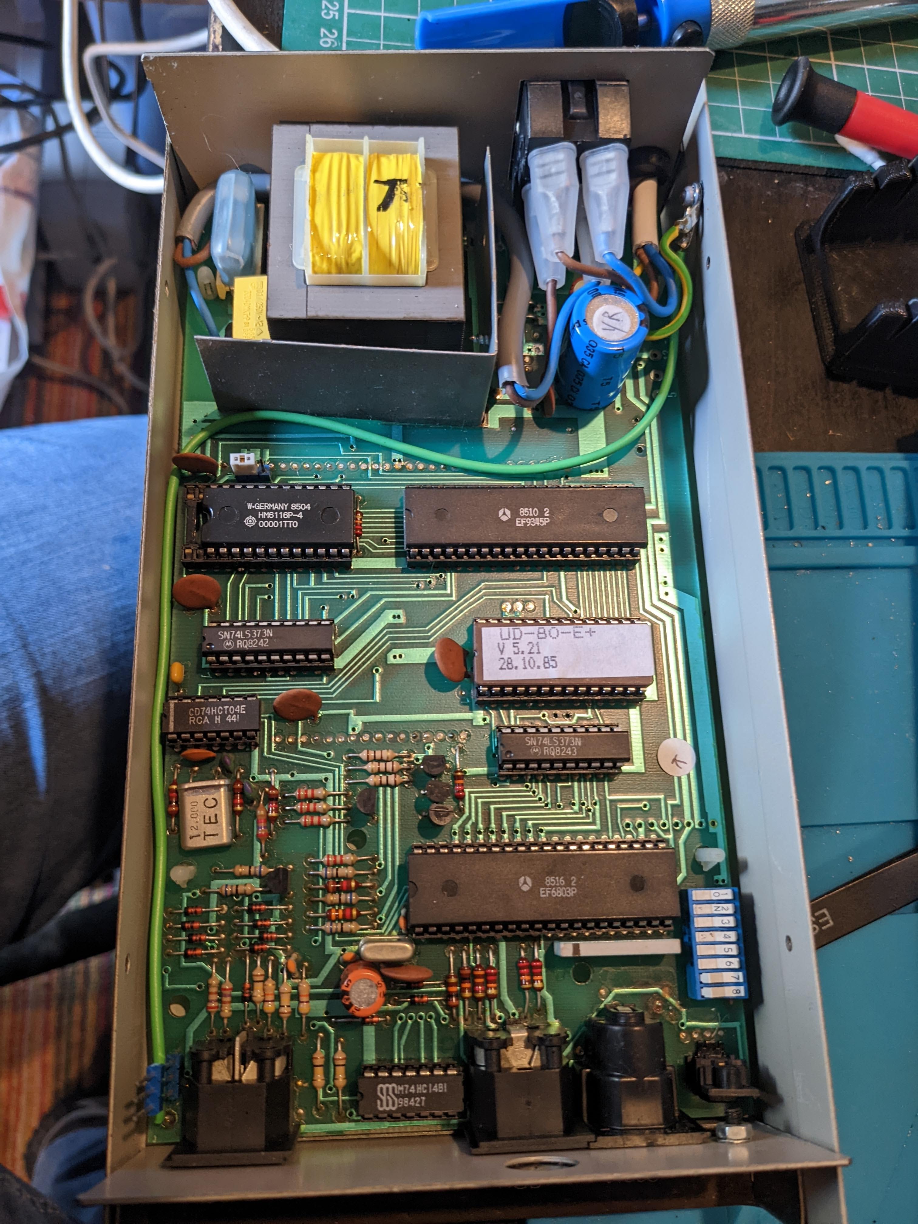
Opening the thing up shows a fairly chunky transformer which makes a period correct 'buzz' when switched on. It also means I need to be careful about touching anything that could make me very sad while it is on.
What's in the box??
Inside there is a Thompson EF9345 'semi-graphic microprocessor' that can generate 8 colours with 128 alphanumeric characters along with 128 'graphic' characters. By todays standards it's vey primitive, but for 1985(ish) it was a definite improvement over the PX-8 LCD display. Also inside are an EF6803 8-bit microprocessor, derived from the 6800 (the Dragon 32 used the 6809 of similar stock).
The question is, does it still work? After a couple of quick electrical safety checks I plugged it in and turned it on. No bangs or flashes. No magic smoke. So far, so good. Now to see if anything was actually coming out of it. So I took my oscilloscope and probed the 'Video' output.
Is this a video signal I see before me?
With the scope showing what looked like a video output I went looking for a cable and found one in the bin (really) with the correct aerial plug on one end and phono on the other and plugged it into the back of my tiny Sony TV.
Yes! A video output! A very SMALL video output!
Success! But its a bit small. As it's composite I tried plugging it into my recovered laptop LCD panel. The composite on the control board isn't the best but it is much bigger than the Sony TV and it's clear to see that the unit is up and working.
That's bigger.
Then I hit a snag. In the huge selection of cables I'd been given with the PX-8 I didn't have an 8-pin DIN to 8-pin mini-DIN that I would need to connect it to the UD80.
After a lot of detective work i.e. I found a 5-pin DIN to 8-pin mini-DIN that is used to connect to DS8 to the PX-8 (did I mention the DS8 yet?), I think I have managed to establish that out of the 8 pins on the UD80 DIN connector, only five are actually needed. These are:
Gnd
RxD
TxD
DTS
DSR
I did think that I could make a 'straight through' cable with all the parts I have, but a quick investigation of the port on the front of the UD80 revealed that pin 2 is GND. This is NOT the same as pin 2 on the PX-8 which is actually TxD. Other 5-pin DIN applications seem to fairly consistently use pin 2 as ground so the UD80 is possibly still wired up a standard way. I just don't know which of the other pins are which. Dangnabit.
But there's another issue. After an initial panic that I did not have the relevant driver file available for the PX-8 (which is called UD80-DRV.COM) I realised, after a couple of people prodded me, that this file is already in the ROM on the UD80 and using the FILINK app on the PX-8 I should be able to get it to download. I even checked that it is by dumping the ROM and having a look!
ROM Dump
Sadly, even though I can run FILINK I have no idea what I need to do to prompt the UD80 to download the driver. I have tried probably a few hundred combinations of the cables into the UD80 with limited success (although it does display some garbage with some combinations) but without the actual instructions on what to do in FILINK it's all a bit moot. Sad face.
Garbage - but it's displaying something!
UD80 end with 8-pin DIN to breakout
Breakout with one of hundreds of combinations installed
PX-8 end
But, on the plus side, I have something that is so incredibly rare that if you search for it on Google, a lot of the top results are my posts on Twitter! And it does look like it would work, if I could find the step by step instructions..
One to re-visit.
More photos for anyone Googling:
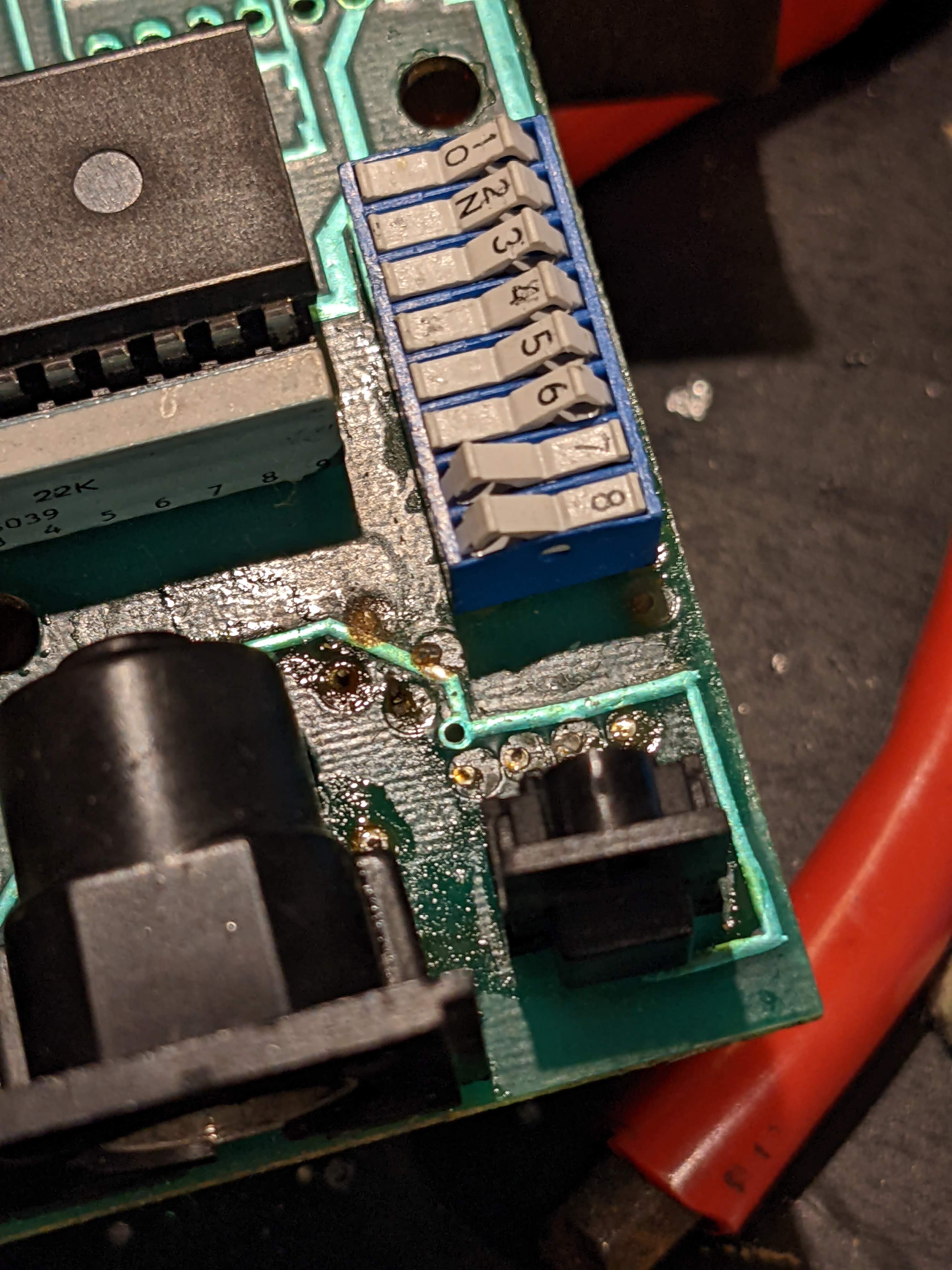
DIP switches - changes things like 40-col or 80-col mode, background colour etc
Connections through DS8 switching box
EEPROM, video controller and 6803 CPU
Bottom of UD80 board
8-pin DIN lower left of board
Video RAM upper right of board
RGB Connector centre bottom of board
DS8 Switchbox with a bit of a design flaw! Case screw screws into the cap!
With my escapades ongoing with the PX-8 RAMDisk you'd be forgiven for thinking that the thing is cursed. Of course it isn't because a) it was free, nothing that is free can be cursed, and b) curses aren't real.
The PX-8 has two slots for ROMS. The ROMs fit into little carriers that I shall call pods because it sounds cool to say 'ROM pod'. So there. These pods contain additional applications to run on the PX-8 which could be anything from a word processor such as WordStar to a diary or calculator. The pods can also accept EPROMs of different capacities and this unit came with a bunch of them.
Pod, pod, pod.
Pod, pod, pod, pod, you get the idea.
The first thing to do with these is to dump the ROMs so that I can re-use the chips for other things but easily restore them to their original state if I need to. This is particularly important for the DS8 video output boxes that came with the PX8 which are probably the rarest things I currently have in my collection. (I don't know if they work but if I don't plug them in and turn them on, they might..) Reach for the Dataman S4!
I'm not sure if I mentioned but I modified the S4 to run directly from a mains adaptor by hooking up the battery terminals directly to a modern power supply. This removes the need for an internal battery which also removes the risk of a damaging leak but has the drawback I have to re-load the 'library' of supported EEPROM devices every time I want to use it. A minor inconvenience.
To get going I just boot up the Dataman software from 2003, which works flawlessly with Windows 10 if you were wondering, and just select 'Download Library'. Then I select the library file, which is still available from the Dataman website, and then wait a couple of minutes. A message 'START LIBRARY?' appears on the display and by pressing 'ENTER' everything is ready to go.
Library 3.00 ready for action
To select the correct chip type it's a simple matter of pressing 'PROM' then using the up/down arrow keys to find the right manufacturer then the left/right arrows to select the right chip. Easy peasy.
This EEPROM is a National Semiconductor.
So, what to do. I take one of the dumped EEPROM chips and a PX-8 ROM file downloaded from the most excellent resources located here and here. How do I get it on to the chip? Well, first of all this is a UV erasable EPROM so I can't clear it with the S4, I need some other way. The datasheets for EEPROMs will normally give an indication of what's required and in most cases it's a blast of UV light at a wavelength of 257nm (nano metres) for about ten minutes.
Intel D27256 EEPROM Note the window where UV enters
I have to tell you now that the EEPROM erasers that are available on various auction and other retail sites are complete garbage. I shall quote from one review of a unit that someone purchased from a well known site:
"This is basically a 'use at your own peril' device. It's really badly made with gaps all around the base and top cover. I'm sure if Her Majesty's Customs had anything to do with this, they'd incinerate them on sight. ... although it feels as if there's a reasonable chance they would do that on their own.
The warnings that come with this are crazy; maybe because they're in broken English. The gist of it is 'turn it on, run and don't look back'. ... Having read the other reviews , the first thing I did was take it apart and put in a new power cable and a fused UK plug. The one you're replacing is terrible - there's around 5 threads per core. ... After leaving on for seven minutes (with an extension lead going to the device, which I sat in a bucket with wood over the top. If I had an x-ray screen I would have probably gone behind that too) it did actually blank the AMD 27C400 inside.
I didn't really doubt that it would, I just expected it to explode or at the very least start smoking as soon as I flicked the power on.
So? If you need to blank an eprom or two, then go for it, but, take enormous care with this piece of junk."
This was not what I would call a 'glowing' review.
But there is an alternative. In a bizarrely 'Hitch Hikers Guide' turn of events, I purchased a 'Phone Sanitiser'. This is basically a white box that you put your mobile phone into and, for ten minutes, it bathes your phone with UV light at 257nm, to kill bacteria and leave you with that smug feeling that you won't catch any virulent diseases while posting cat pictures on Instagram (or whatever the kids are doing these days).
You won't be wiped out by a virulent disease contracted from a dirty telephone.
But did you see what it does? It emits 257nm light for ten minutes. And it only cost me £13. And it's a surprisingly high quality unit. There is mention of 'Samsung' on the box and in the small manual it comes with but it's not directly made by Samsung. No matter. It does what I need it to do.
Opening the lid reveals two small tubes, one at each end. By resting the EEPROM with the window directly facing the tube, it is completely erased in ten minutes. Blank EEPROMs are full of 'FF's which indicates they're ready for writing. Nice. I shall probably look at designing and 3D printing something to hold the chips more securely in sanitiser in the future.
Open sesame..
FFs sake.
So now I have a blank EEPROM and I want to write my downloaded ROM to it. In the S4 software I just select 'Transfer > Send file (PC>S4)' and select the ROM file. The format of the file can vary, mine is a 'HEX' format, but the software supports at least four different formats.
After a minute or two the transfer is complete and on the S4 software I select 'Memory>Checksum RAM' to check what the value should be, then 'Device Pretest' which should tell me the EEPROM is blank. Then I can 'Burn' which copies the contents of the S4 RAM onto the EEPROM. Once complete I always do a 'Device>Checksum ROM' to make sure it matches the RAM checksum from earlier.
In theory, the EEPROM should be ready for installation into the bottom of the PX-8. The little carriers aren't essential and the EEPROM can be fairly easily pressed into the socket without any problems.
Does my new ROM work?
Yes. (Sub Zone)
Yes. (Tower)
Yes. (Tank Attack)
Yes. (Snake Pit)
These are about the only games for this system (I do have a version of Othello I want to try though) and they all work perfectly and are surprisingly fun, even if my aged hands start to hurt on the cursor keys after a few minutes.
Before the shenanigans with my oscilloscope I was busy trying to repair the faulty PX-8 RAM Disk.
I was in the process of testing all the chips. And I have actually finished testing them all now. All chips are now working, either as their original chip or with a replacement. I managed to also check the EEPROM by using the S4 Dataman EEPROM programmer to dump the ROM and compare it with a version obtained online from the most excellent PX-8 resource located here.
Here's my spreadsheet (everyone loves a spreadsheet):
Chips.
Sadly, however, even with all of the chips installed, the behaviour is unchanged and the PX-8 screen sits with a sad cursor, flashing on an otherwise blank screen.
Very quickly, I noticed something a bit strange. If I probed pin 2 or pin 14 of chips 17A or 17B (although only 'A' is populated for 60kb mode), the resulting wave was very dim and unstable and would suddenly revert to no signal, as if there was a 'crash' occurring on the board.
Interesting. Very interesting.
The pins 2 and 14 are the DI (Data In) and DO (Data Out) pins on the RAM chips. For each chip (actually pair of chips e.g. 17A and 17B) the DI/DO pins are tied together. This does sort of make sense since the data on that line and its direction is also dependent on other signals so if data is heading into the chip it is irrelevant if that data appears on the DO pin, and conversely, if data is being read from DO it cannot be read into the chip at DI unless the 'Write Enable' pin is also active.
And since there are eight RAM chips (or eight pairs with bank switching) this means that each chip/chip pair is looking after one bit of RAM. In this case, chips 17A and 17B look like they are looking after data bit '7'.
So, where does this combined line go to? Well, it goes to chip 9B (a TC40H374P flip flop) at pin 19 and is a 'Q' input. It also goes to chip 8B (the other TC40H374P flip flop) at pin 18 which is a 'D' input. But it goes further. This line also goes straight to pin 13 on the Z80A which means that this line is confirmed as being specifically for data line D7. And it also heads over to pin 16 of chip 11C which is a bi-directional driver. Finally, it also runs to pin 17 of the EEPROM.
To check whether this line was fully connected was a simple case of doing a continuity check across the various points and pins on the right chips:
Pin 2/14 to pin 19 on chip 9B - CHECK
Pin 2/14 to pin 18 on chip 8B - CHECK
Pin 2/14 to pin 16 on chip 11C - CHECK
Pin 2/14 to pin 17 on the EEPROM - no continuity
Pin 2/14 to pin 13 on the Z80A - no continuity
At this point I thought I had found the problem, a broken trace that prevents reading/writing of data bit 7! Yes!
But. No.
Before I started soldering wires anywhere I just so happened to run the multimeter probe up and down the legs on the EEPROM. And guess what I found? Data bit 7 doesn't go to pin 17 on the EEPROM. It goes to pin 19. And pin 19 on the EEPROM connects to pin 13 on the Z80A. I appear to have found an error in the technical manual of this thing. Or possibly a different board revision. Or it could be that the pin allocations are just different depending on the EEPROM version (but would still need a different board layout).
Arse.
Back to square one.
Today I decided that I would re-flow the solder joints on the 'Gate Array' chip (I shall call him Gary) since this is the only chip that is not in a socket and is surface mounted. This escalated into a complete removal and re-attachment. Definitely not a fun 45 minutes. Although this chip is quite chunky with fairly big legs for an SMD chip, it's at the absolute limit of my soldering ability and I just about managed to do it without lifting any pads. The re-attachment is not pretty but the legs are all connected as they should be.
Gary removed..
Sadly, this activity appeared to confirm my worst fears. After removing Gary I plugged the RAM board in and the results were exactly the same as before i.e. a sad, lonely cursor flashing on a blank screen. After re-attaching it, the results were again the same.
This says to me that it's 99% certain that Gary is dead. Poor Gary.
These units are pretty rare so this means that Gary is the purest form of unobtainium.
But I refuse to give up!
So, let's do some more continuity checking. This time, I shall focus on the pins of Gary and the destination of all 80 of those tracks. I feel another spreadsheet coming on!
Gary re-attached - not pretty..
Two spreadsheets in one post. I'm spoiling you.
After a couple of hours I had discovered a couple more things. Firstly, two pins on Gary had not been soldered on properly and were still loose, most importantly pin 45. Secondly, there is no continuity between pin 45 of Gary and pin 8 of chip 11C. This remained the case after I had carefully re-soldered pin 45 back to the board.
Attaching a jumper wire from pin 45 of Gary to 11C was straightforward enough, but, again, this made no difference at all.
Bodgit and scarper..
On the plus side, with my newly repaired oscilloscope I began to poke around the Gary pins and found sensible looking outputs for a gate array. So perhaps Gary isn't as dead as I thought.
I am getting desperate with this now. My next step is to de-solder all of the original RAM sockets and check for unseen damage under the board. Then, I shall replace the few through hole resistors that are on the board (one looks to have caught some battery leakage quite badly) and consider doing the same to the four or so transistors.
Or I might just put it away for a while and think about other things...
Parts have started to arrive for the planned repair of my oscilloscope. I will document what I do here, and try and do it properly so anyone who has the same problems or needs to replace the HV tripler in this type of oscilloscope might stand a chance, based on my success (or failure) to do the same. Some information here is duplicated from previous posts.
The oscilloscope in question is badged as an IsoTech ISR441 40Mhz scope. I believe that these were branded by RS Components in the late 80's and early 90's. Following the research and lucky finds I had on the internet I can identify that the model I have is a re-badged 'Hung Chang' 5504 40Mhz oscilloscope. The link to the manual can be found here from the EEVBlog forums. (If this stops working leave a comment and I'll see if I can fix it.)
Hung Chang 5504 40Mhz scope
The problem I had with the scope is basically it now has no trace. Prior to the trace disappearing I had noticed that it had started to become dim, but only sometimes. Once it was dim it would sometimes go back to being bright again, sometimes it would not. Changing the controls had no real affect that I can speak of. One day, the trace was bright as normal, and the scope was on. After a few minutes I turned to use it and the trace had disappeared.
Switched on but no trace
Checks revealed that the test signal on the front still works and power supply rails are at the correct voltages.
Inspection of the board with the HV circuit (there are two main boards in the scope - the one in question is the board mounted on the side of the scope) revealed that there were apparent burn marks on the HV tripler unit at the point where the Anode cable leaves the unit. There were also signs that the plastic case had started to melt and had expanded and 'bubbled up' in some places.
Burn marks close to Anode cable
Deformed plastic case
Removal of the HV tripler from the circuit board also revealed a large hole in the plastic with evidence of the expulsion of burnt potting compound onto the heatsink of a nearby power transistor (Q2001).
Hole in faulty tripler
Q2001 heatsink shows the material expelled from the faulty tripler
This scope makes use of a separate Flyback Transformer and HV Tripler unit rather than the more conventional combined units as seen in CRT TVs and CRT based computers such as the iMac G3.
Page 37 of the manual shows the circuit diagram for the voltage tripler unit. These units are not manufactured and so the only option to repair this scope is to build a new tripler from discrete components using the parts list and circuit diagram as a guide.
Tripler circuit diagram (page 37 of manual)
The components required are:
6 x 1000pf 6kV ceramic capacitors
6 x Y-16GA or equivalent 10kV high voltage diode (typical forward current 5mA)
1 x 1/2W 10M ohm solid resistor
The components I have purchased are:
6 x 1000pf 15kV ceramic capacitors
10 x 10kV diodes
2 x 1W 10M ohm resistors
Note that the ratings I have may differ from the service manual. This is primarily due to availability of components, especially the capacitors. Note that in most cases it is acceptable to pick a voltage rating higher than the original component.
Capacitors and 1W resistors
I will also be making use of the original Anode cap and cable. To contain the unit, once constructed, I have 3D printed a small box that matches as closely as possible the dimensions of the original ABS box. This initial 3D print is made with PLA which, despite being an excellent insulator at room temperature, begins to lose its insulating properties as its temperature rises towards 65 degrees celsius. As such, I would not recommend PLA for the final box since it sits very close to the heatsink for the large power transistor Q2001 - a D880. Using ABS instead of PLA will provide a more suitable box since ABS has a much higher 'glass transition' temperature i.e. the temperature at which the plastic starts to become 'rubbery'.
In my case the PLA box will be used to evaluate whether the constructed tripler fixes the oscilloscope and, if so, a more appropriate container will be procured/constructed/printed.
Two sizes of replacement box
Q2001 and Heatsink (Note proximity of tripler box outline)
Space is very limited within the confines of the board and the fly-back arrangement is also covered by a silicone (or rubber) lined aluminium cover. I intend to use the space as the factory unit did with the 3D printed box, if possible but it will be tight due to the number of components required to build the unit. If the aluminium cover is to be retained, which I very much hope I can do, the potential for going beyond the original unit size is very limited due to the mountings of the two main boards.
Aluminium cover - limited access
Tripler Construction
To start, I laid out the components that I have in a rough pattern of where they would sit. Note that in this picture I was still waiting for the final delivery of diodes to complete construction. As such, the final diode is missing from this picture which would connect from the top right most diode to the resistor and capacitor bottom right.
Rough Layout
First, I soldered the two groups of three capacitors together, making sure to leave a small amount of leads between the caps so that I had something to connect the diodes to. Then I twisted alternate ends of the diodes together to make an extended 'W' shape, being sure to put the cathode (the end with the markings) pointing in the correct direction. Following the circuit diagram, with voltage coming in from the left, the cathode marking was on the 'right' of every diode following through the ladder.
Once this was done I soldered the legs of the diodes to the gaps between the caps. This resulted in the following:
Partially constructed
Due to the limited space in the box, I put the caps so that they will be at the bottom of the box with the diodes connected on top. There is also a 10M ohm resistor that is the final component before the cable that runs to the anode cap at the CRT.
Resistor added to end of Anode cable
The leads of the first two caps are long enough to extend down through the bottom of the box and into the correct places on the circuit board i.e. the two holes at the 'In' end of the tripler outline. The two holes at the 'Out' end of the tripled are only used for anchor points (an assumption) as they both appear on the ground plane underneath and the actual 'out' voltage is the anode wire and cap.
Tripler location next to transformer Note 'In' and 'Out' markings
I intend to to use a 'u' shaped piece of silver wire to perform the same anchor function in the 3D printed box I will use. In the picture above the space for the tripler has two holes on the left which are the ground 'anchor' points, and two holes on the right. The hole nearest to the transformer (top) is also ground. The hole at the bottom is the 'in' voltage that arrives from one side of the flyback transformer.
Completed construction (note second diode has become disconnected)
Following completion of the tripler, I installed a small piece of silver wire to support the box at the end where both connections connection to ground. Next, I placed small pieces of heat-shrink on the joints of the capacitors to try and reduce the potential for arcing between the components due to the high voltage. Then I slid a large piece of heatshrink over the end of the anode cable before soldering the end of it to the final diode/cap joint in the ladder.
With this done I slid the whole thing into the box, lining up the two legs of the first section of the ladder with two holes I made in the bottom of the box. These holes line up with the 'in' and 'ground' connections on the 'in' side of the tripler. Finally, I put a piece of insulating tape over the top to hold the cable in.
I have some concerns with this very temporary design. First, I don't know if my efforts to insulate the components have gone far enough. Ideally, the whole thing should be potted into the box. BUT, as mentioned above the temporary box here is made of PLA and is not ideal for scenarios with temperatures over 65 degrees celsius and so it will be replaced. Potting it would make box replacement almost impossible without re-building it all over again. Second, the final 10M ohm resistor presses up against the PLA. I don't know how hot it may get and so I am wary of leaving it in there since, if it gets too warm it may melt the PLA exposing the resistor to potential arcing targets.
So, this arrangement (as shown below) will at least show if this is going to work.
Assembly complete Ready for installation
Re-installed on the board.
Awaiting main unit re-assembly
Re-assembly of the oscilloscope was a reverse of disassembly. There were three wires to re-solder into board, one brown wire (connects to a BNC connector on the front panel) and the two wires that drive the CRT 'x' deflection. I had to be careful soldering these back in as the pads on the board started to lift when I removed the cables originally.
All the screws were re-installed and the plastic cover re-attached with the black pegs holding it in place. The cover is important as it offers some protection against accidentally touching the high voltage section of the board - so not to be left off! The numerous connectors were re-attached with their positions being fairly obvious due to the orientation and natural position of the various plugs, so there were no issues there. A couple of them are deep inside the centre of the board and I found a long pair of tweezers were helpful in getting these re-connected.
The main power cables were re-connected to the board and these were the only connections I hesitated on as I realised I did not have a good photograph of them pre-disassembly. I verified that I had them correct by checking the connector orientation and voltages in the manual.
Re-attaching the CRT neck board was straightforward as the connector is keyed and will only sit flush if attached correctly. Finally, the anode cap was re-attached to the CRT.
This is now in a suitable condition to try a switch on.
Ready for test run
To ensure maximum safety I plugged the unit into an extension cable and then took it and placed outside of the garage door. The thinking being that in the event of a catastrophic failure the damage would be limited to my garden and not the garage and its contents. In addition, I took the added precaution of using a piece of wood to turn on the main power switch.
And the result was... a working oscilloscope. This is a fantastic result but not the end of this project. As mentioned above I intend to 3D print an ABS box which will be far more heat resistant that the PLA one currently installed. Once that is done, which will require another disassembly and re-assembly, then I will move on to the calibration process which, thankfully, is well documented in the manual.